 CastrLab

Full disclosure, I have no connections to Framework. I just think it’s a product worth supporting.
I found myself in the market for a new laptop a while ago. I can’t recall how I learned about the Framework Laptop, but the idea of it was too interesting to pass up. The crux of the platform is a modular-based laptop which offers upgradeability and repairability. As a perfect example, the laptop I originally purchased came with a motherboard issue; After getting a replacement motherboard, the swap took less than 15mins and with a single screwdriver. While the ability to repair and upgrade alone is worthwhile and enough for me to put my money where my mouth is, the part that really sparked my interest was the removable expansion modules.
On a regular laptop, you have your predefined peripheral ports. If you’re lucky, a couple of USBs, an HDMI, and maybe an Ethernet. Instead, the Framework laptop has these small rectangular modules that slide into the chassis and connect over Thunderbolt 4. Currently, the company sells eight modules, including expandable SSD modules, but encourages the community to design their own.
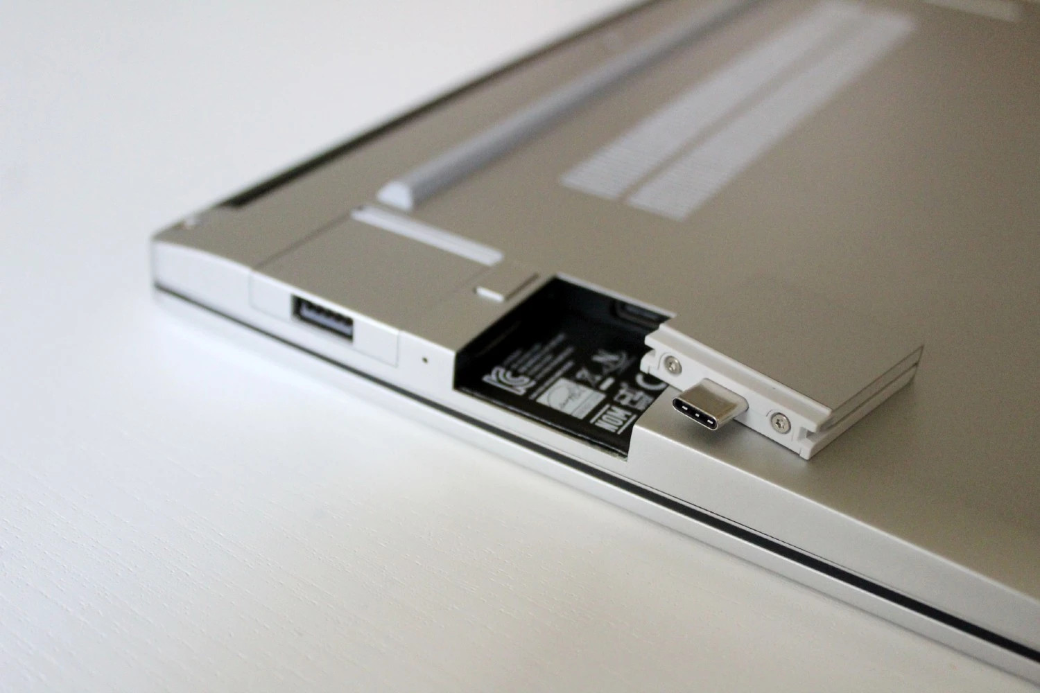
This concept got me thinking about my work and the tools I could integrate into these modules, power supplies, volt meters, logic analyzers, etc. Provided the front-end hardware can be miniaturized, the laptop’s CPU takes the computation parts. So began my journey to build a multi-protocol serial bridge.
The design requirements were fairly simple and limited.
- All components must fit within a board size of approximately 20mm x 20mm, preferably all on one layer, to make hand assembly easier.
- At a minimum provide basic I2C, SPI, UART communication
- Simple LED status and data indicators
- Must be able to transmit and receive data at 1.8V, 3.3V and 5.0V
- Everything must be able to run off a maximum of 500mA. This one is a soft requirement since USB-PD allows for up to 3A.
Version 1
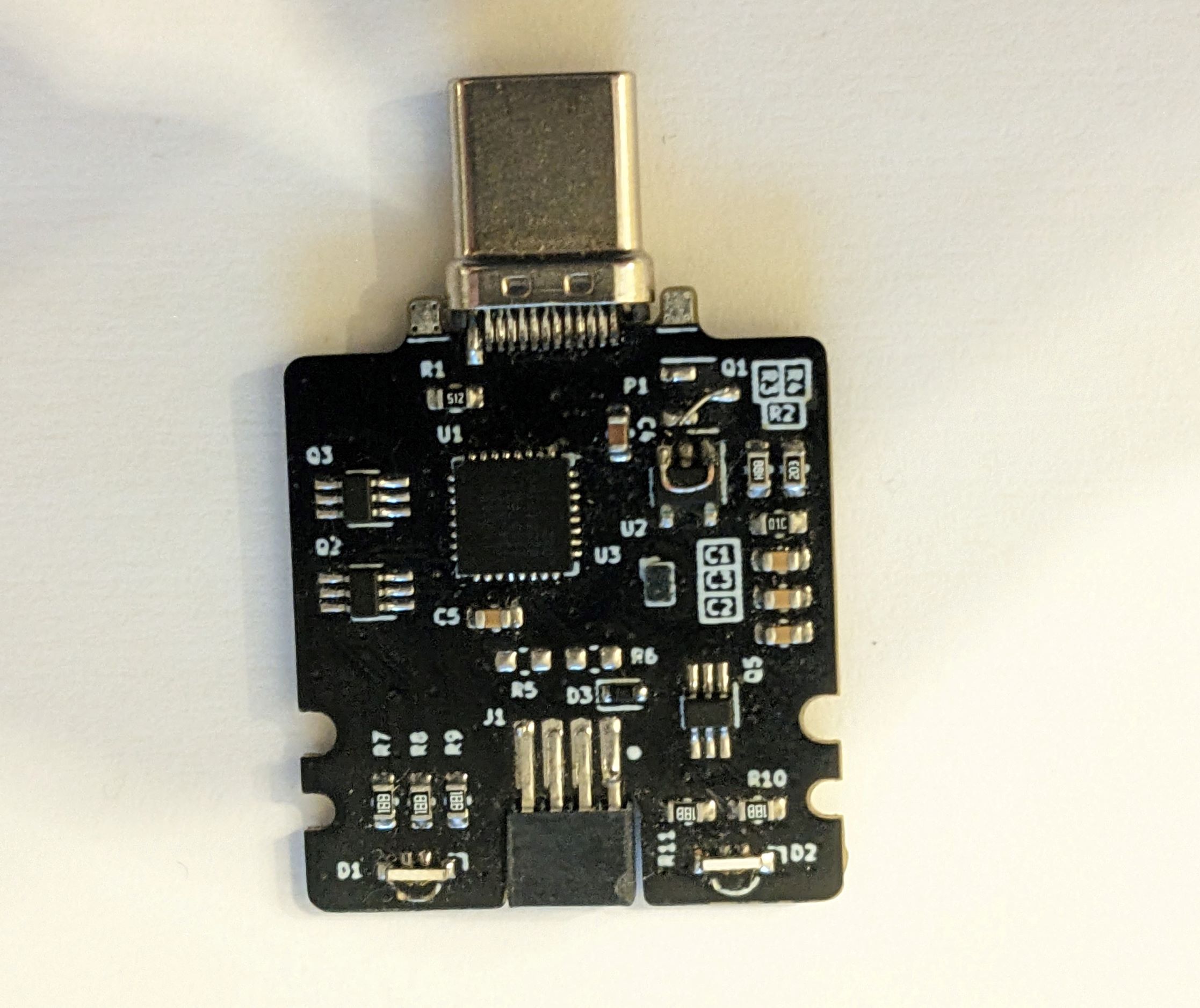
On the first attempt, I thought, “go simple” and go for an integrated USB-serial bridge. Typically, you can find a single-chip solution that offers all the protocols I’m looking for and some additional GPIO pins. The CY7C65215 was a great place to start since it had several GPIO pins and all the interfaces I needed, plus JTAG, which could come in handy down the line. Additionally, the CY7C65215 has a dedicated voltage pin to power the IO; adjusting the voltage on this pin would allow me to hit all the logic levels I wanted to.
Power
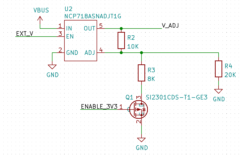
With the bridge selected, I needed a way to control the IO voltage in discrete steps programmatically. Programmable Linear Dropout Regulators (LDO), like the MAX8902A, allow you to control the output voltage through several digital control pins. Still, these parts are prohibitively expensive, harder to find reliable stock or have footprints much larger than your standard adjustable LDO. Instead, the idea was to take a standard adjustable LDO and create an adjustable feedback network using two parallel resistors and a MOSFET. By switching the MOSFET on and off, one of the resistors can be removed from the feedback path and change the voltage set point.
That puts the 1.8V and 3.3V, provided by the LDO, in one power domain and the 5V USB VBUS in a second. I still needed a method to switch between the two domains in such a way that provides an uninterrupted transition. If power is lost to the pin that supplies the IO with power, the module will be stuck in one domain or dead in the water.
One method typically used in systems with more than one power supply is a back-to-back MOSFET configuration. There are several articles on how this circuit works, so I won’t be going over it here. On top of this, I’ll need an inversion circuit to ensure one pair of MOSFETs are on while the others are off. The back-to-back configuration is a perfectly adequate design choice. Still, I’ll need a smaller solution due to my space constraints. Instead of using the five MOSFETs, I’ll use the FPF1320 2:1 power multiplexor at an absolutely microscopic 1.4x0.96mm, with more than enough power allowance and built-in seamless transitioning.
Interface
For the interface, the idea was to write an application that would be able to reconfigure the CY7C65215 on the fly using their API, similar to the configuration tool Infineon provides for the device. As it turned out, this wasn’t possible. The API didn’t support configuring the device, only accessing the internal register. To configure the device, I needed Infineon’s proprietary tool. There was a workaround, but it required generating a configuration file for every possible configuration and uploading each as needed using a combination of their encryption tool and my UI
In hindsight, this was a fool’s errand. Writing an application like this would eventually require providing software support across various platforms and operating systems; honestly, that was not something I wanted to do.
Version 2
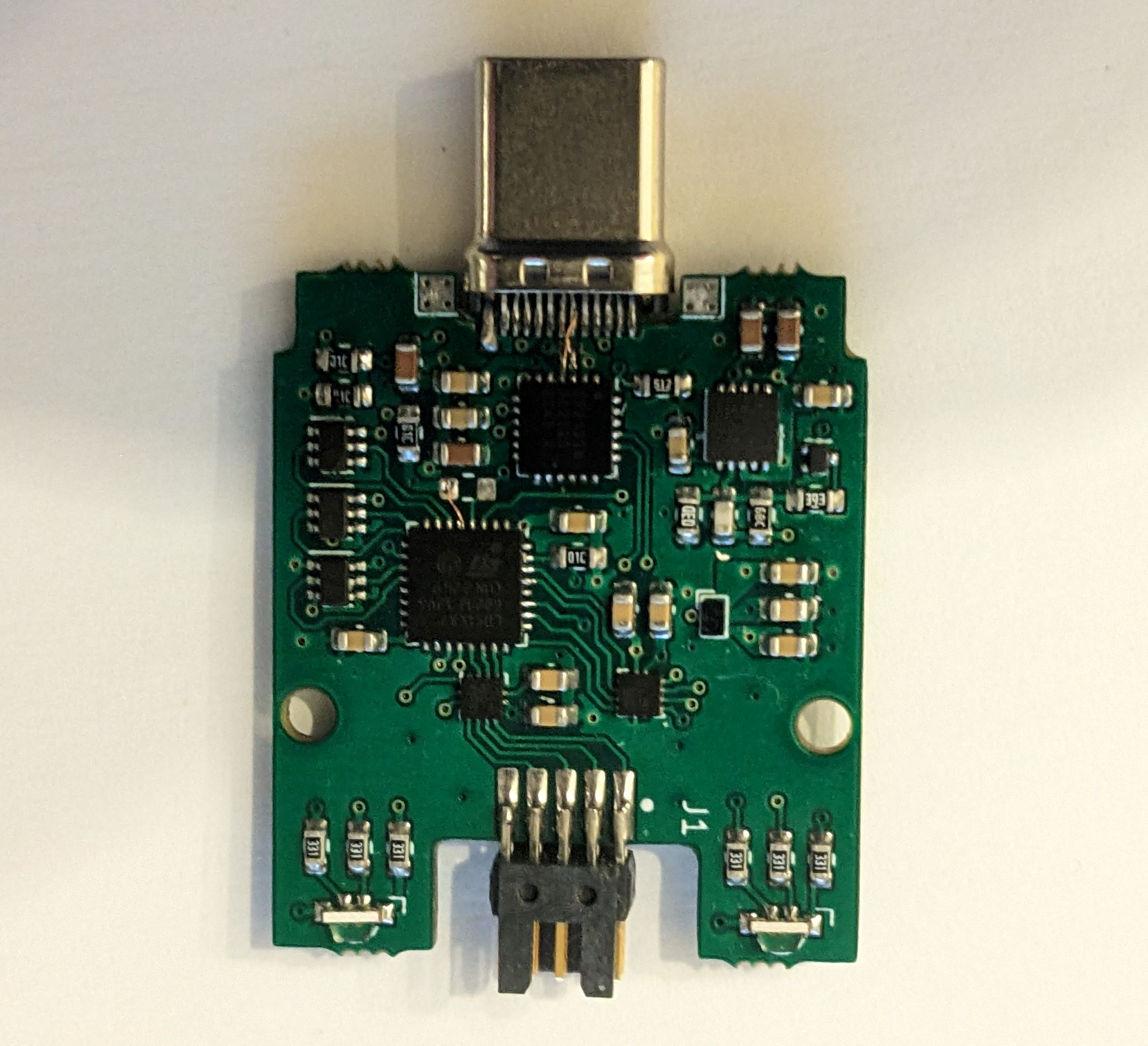
Instead of trying to fix the shortcomings of the serial bridge and maintain a code base well outside my experience, I opted to cut my losses and start with a new design concept. Since the inspiration for the project came from the Bus Pirate, I decided to take a page from their book and use a microcontroller solution instead.
MCU Interface
Ultimately using a Microcontroller Unit (MCU) is the superior choice for a few reasons. First, The console software will be built into the device and, therefore, compatible across all platforms with a serial terminal. There will be no need to write custom software and drivers for windows, Linux and Mac, which “should” allow for quicker development. Secondly, an MCU allows additional features not built into a typical serial bridge. Using the different built-in peripherals, I can use input captures to measure clock frequencies or monitor control lines with unused GPIO pins.
One of my considerations for the MCU was it must be easily programable in that no additional hardware should be required. The module will inevitably need updated firmware, and I would prefer not to remove it from its case and solder jumper wires every time I need to tweak somthing. The STM32 line of MCUs comes with a bootloader that only requires a UART connection. So. Since I’m already relying on a USB-UART terminal to communicate with the device, this was a perfect feature.
Level Shifting
Unlike the previous design, the MCU doesn’t let me control the IO voltage directly, or at least not the pins I want. Instead, I’ll need to add an external level-shifting circuit. I could have built a simple level shift circuit with a MOSFET and a couple of resistors. But, again, my design choices are space limited, so I’ve opted for an intergraded solution. Because the level-shifting circuit will have a fixed high and low side, I can’t shift a 3.3V signal up to 5V and down to 1.8V. This has established the second selection criteria for the MCU. I’ll need to select one with a minimum operating voltage of 1.8V to shift IO signals to higher levels.
Power
With the first design, since the serial bridge could run off 5V from the USB and the IO off the adjustable LDO, I could get by with a single LDO. This time, I’ll need a third 1.8V fixed voltage domain for the MCU and serial bridge on top of the 5V and adjustable IO domains. Instead of dropping down a second LDO, I chose a dual-channel device with one of the outputs fixed to 1.8V to reduce the component count.
Aside from that, the design remains relatively unchanged…
One day, after I’ve worked out the firmware and the inevitable hardware bugs, I might sell a few to help fund further development on future modules. But for those who want to expand on my work or build your own, I’m making this project public in the spirit of right-to-repair and open source hardware.
Gitlab link